 TheTechMedia.com/wp-content/uploads/2022/02/27325956508_d89a33a51c_b-300×222.jpg 300w, https://TheTechMedia.com/wp-content/uploads/2022/02/27325956508_d89a33a51c_b-768×568.jpg 768w, https://TheTechMedia.com/wp-content/uploads/2022/02/27325956508_d89a33a51c_b-800×591.jpg 800w” sizes=”(max-width: 1024px) 100vw, 1024px”>
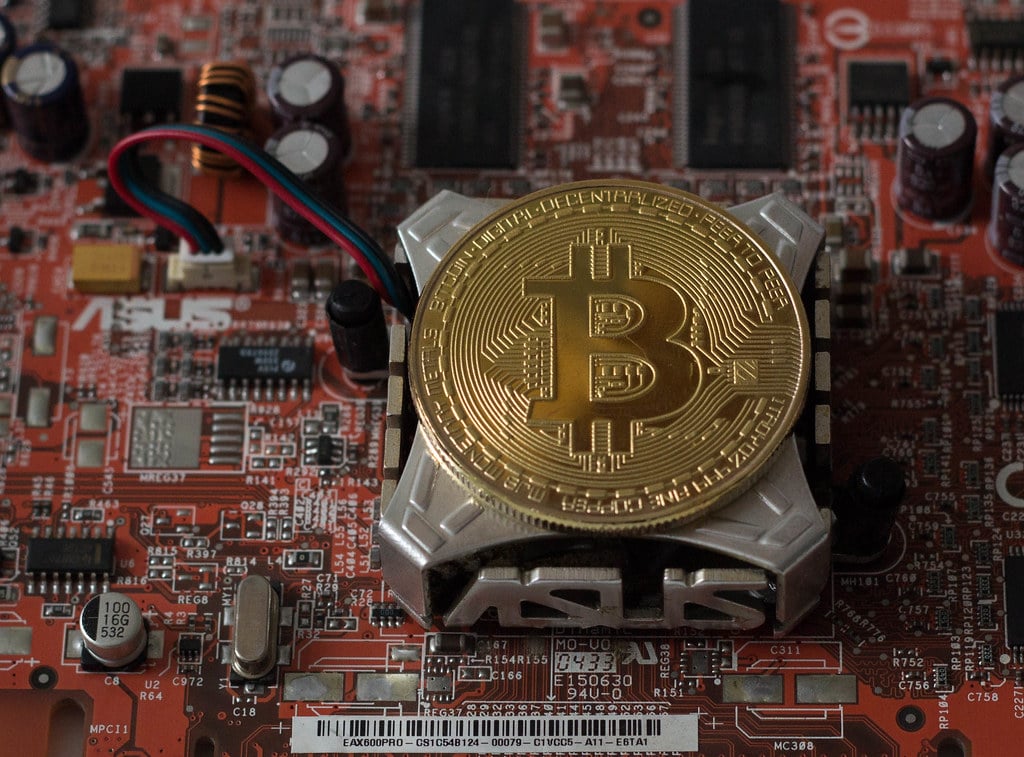
The process of mining Bitcoin is complicated as a massive computing system, electricity, and expensive software work together to generate new units of cryptocurrencies. As Bitcoin and other cryptos have soared (but soured in terms of price in recent times) over the past year, there arises a need for something to ease the process of Bitcoin mining.
Intel’s Bonanza Mine (BMZ1) is aimed to do exactly that, and now, the company has shared more details about its blockchain accelerator mining chip.
At the International Solid-State Circuits Conference (ISSCC) this year, the American multinational company shared more details for the first generation of the Bonanza Mine blockchain accelerator chip, the same which promised 1000 times better performance per watt of energy than a traditional GPU.
To talk more about the BMZ1, it is an application-specific integrated circuit (ASIC), which means that it is designed to carry out specific tasks. In this case, the task is mining Bitcoin using the SHA-256 hash algorithm. The process is slated to save more energy. Alongside, Intel also unveiled a new 3,600-watt mining rig with a system hash rate of 40 terahashes per second (TH/s), comprising entirely of 300 BMZ1 chips.
The BMZ1 leverages the 7 nanometers (nm) process and a die size of 7 x 7.5mm exposed-die FCLGA package. Each chip die measures 4.14 x 3.42mm for a total of 14.16mm2 of silicon, and the smaller die size helps to maximize production capacity. This is possible since it improves yield and maximizes wafer area usage (where a single wafer can have up to 400 chips).
Intel claims that its BMZ1 chips are the cleanest and most powerful on the market. Whether it is true or not remains to be seen, but the fact remains that it has already received orders for the BMZ1 from Block (formerly known as Square and founded by ex-Twitter CEO Jack Dorsey).
Intel will not stop at the BMZ1 blockchain accelerator chip and has already started working on the second-generation BMZ2, also known as the Bonanza Mine ASIC. It seems that each Bonanza Mine ASIC has 258 mining engines, and each engine computes parallel SHA256 double hashes.
These engines comprise 90% of the die area and operate at what Intel says is an ‘ultra-low’ voltage of 355mV. Each ASIC operates at 1.35 to 1.6 GHz at 75C, consuming an average of 7.5W apiece while hitting up to 137 Ghash/s. That works out to 55 J/THash/s at 355mV. It seems that it has already attracted the attention of Bitcoin mining company Griid if the S-4 filing is anything to go by.


